Transistor circuits can be daunting for beginning students. It's a big jump in complexity beyond resistors. Some reasons are:
Fortunately for you, the circuits we'll be asking you to work with in 6.002x are artifacts that were designed for a purpose rather than arbitrary bunches of components that happen to be connected together. You can therefore get a hint of how the transistor is operating by making a guess about the intent of the circuit. In addition, since the circuit was designed, the operation of the transistor is will probably be satisfactorily described by a simple model: otherwise the person who designed the circuit wouldn't have understood it enough to design it!2
This note presents a procedure for analyzing circuits with bipolar junction transistors. It's not foolproof, but it's good enough for 6.002x (and much else).
Here's the general form of the procedure:
Now for the details ...
 |
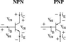
Figure 1 shows the standard symbols for NPN and PNP bipolar junction transistors. The small solid arrow on each symbol identifies the emitter. The arrow faces out to indicate an NPN transistor and in to indicate a PNP transistor. Observe the open arrows indicating the reference directions for the currents: For an NPN they flow in to the base and the collector, and out from the emitter. For a PNP they flow out of the base and the collector, and into the emitter. We've drawn the NPN transistor with the emitter on the bottom, and the PNP transistor with the emitter on the top, so that in both cases the reference direction for current flow is ``down'' as seen on the page. This is a common convention, but watch out for circuits with transistors that are ``upside down''.3
For either kind of transistor, and for any of the models you'll use
below, it is always true that
![]() and
and
![]() , since these are just KCL and
KVL for a three-terminal device.
, since these are just KCL and
KVL for a three-terminal device.
Suppose you need to analyze a circuit that contains an NPN transistor.
For almost all circuits you'll encounter, the transistor is acting either as a switch or as an amplifier.
Do you think the transistor is being used as a switch? If so, it should be operating either in the cutoff region or in the switched-on region, depending on the inputs and on the region of operation of the other transistors in the circuit.
Do you think the transistor is being used as an amplifier? If so, it should be operating in the amplification region.
Using these values, try the amplification region test (step 2b above) and the
![]() test (step 2c). If they work, then this exponential model
was appropriate for analyzing the circuit.
test (step 2c). If they work, then this exponential model
was appropriate for analyzing the circuit.
If neither of the amplifier models work, and the transistor isn't operating as a switch, the either the transistor is intended to be an amplifier and really does become cut off or switched on (maybe the circuit doesn't work or maybe it was really designed to take advantage of this in some fiendish way) or you need to apply a more complicated model of the transistor, which we won't be doing in 6.002x.7
PNP transistors behave exactly the same as NPN transistors, except for
a few signs. Using the labeling conventions we show in
figure 1
![]() as before,
and only the signs of the voltages are changed.
as before,
and only the signs of the voltages are changed.
The PNP transistor turns on at
![]() and it
switches on if
and it
switches on if
![]() , and the equation
describing the behavior of the transistor in the amplification region is:
, and the equation
describing the behavior of the transistor in the amplification region is:
The analysis techniques described outlined here are a distillation of
years of experience. When analyzing an amplifier we try to use the
0.7 Volt infinite ![]() model first because if it is appropriate the
amount of work we have to do is very small. We should never depend on
the
model first because if it is appropriate the
amount of work we have to do is very small. We should never depend on
the ![]() of a transistor being any particular value, because this
parameter is highly variable, both by sample and by temperature.
of a transistor being any particular value, because this
parameter is highly variable, both by sample and by temperature.
On the other hand, the 0.7 Volt drop for a transistor operating in the
amplification region is a
pretty good representation of the transistor to the rest of the
circuit. However, never use the 0.7 Volt assumption with the
exponential equation. The collector current computed this way is very
sensitive to errors in the base-emitter voltage, so the result will be
meaningless. But it is OK to use the infinite ![]() assumption with
the exponential equation.
assumption with
the exponential equation.
To add insult to injury for the student trying to learn about transistors, there is an inconsistent use of terminology describing the regions of transistor operation. Most treatment talk in terms of the transistor's saturation region. Unfortunately, ``saturation'' is usually used to describe different non-analogous regions of operation for Bipolar Junction Transistors and Field Effect Transistors (which you will see soon).
In an attempt to be more consistent, we have chosen in 6.002x to use the words ``cutoff region,'' ``amplification region,'' and ``switched-on region'' to describe the three regimes of operation of a transistor, in a way that is the same for both BJTs and FETs.
However, this requires a mapping to the terminology used in the books we reference:
| 6.002x | BJT | cutoff | amplification | switched-on |
| 6.002x | FET | cutoff | amplification | switched-on |
| Senturia & Wedlock | BJT | cutoff | active gain | saturated |
| Senturia & Wedlock | FET | cutoff | active gain | saturated |
| Horowitz & Hill | BJT | cutoff | active linear | saturated |
| Horowitz & Hill | FET | cutoff | saturation | linear |
| Gray & Meyer | BJT | cutoff | forward active | saturated |
| Gray & Meyer | FET | cutoff | saturation | ohmic or triode |
| Agarwal & Lang | BJT | cutoff | active | saturated |
| Agarwal & Lang | FET | cutoff | saturated | triode |
Note in particular that in Agarwal and Lang, ``saturated'' for a MOSFET is the region where you use it as an amplifier, while ``saturated'' for a BJT is the region where you don't use it as an amplifier.
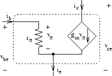
Once we have determined the operating point (the DC bias conditions) for a transistor in the amplification region we may want to understand its behavior as a small-signal amplifier. This is accomplished by building an incremental model of the circuit, with the transistor replaced by an incremental transistor model. An incremental model is linear, so it is easy to work with, and it can accurately capture the behavior in terms of small deviations of the voltages and currents.
One useful incremental model for the transistor is as a resistor and
voltage-controlled current source (see Figure 2).
The parameters of this model are easy to compute. Given the collector
bias current ![]() , the transconductance,
, the transconductance, ![]() , is
, is
![]() . The base-emitter incremental
resistance
. The base-emitter incremental
resistance ![]() is computed from
is computed from
![]() . If we are
working under the assumption that
. If we are
working under the assumption that ![]() then we just set
then we just set
![]() .
.
 |
This document was generated using the LaTeX2HTML translator Version 2K.1beta (1.48)
Copyright © 1993, 1994, 1995, 1996,
Nikos Drakos,
Computer Based Learning Unit, University of Leeds.
Copyright © 1997, 1998, 1999,
Ross Moore,
Mathematics Department, Macquarie University, Sydney.
The command line arguments were:
latex2html bjts-without-tears
The translation was initiated by Hal Abelson on 2004-02-11